World’s Smallest LED Converts Mobile Phone Camera into High-Resolution Microscope
Posted on 05 May 2023
A team of researchers at Singapore-MIT Alliance for Research and Technology (SMART, Singapore) has successfully created the world's tiniest LED. This miniaturized LED is smaller than the wavelength of light, but with a light intensity equivalent to much larger, state-of-the-art Si LEDs and has the capability to transform existing mobile phone cameras into high-resolution microscopes. This was achieved simply by making changes to the silicon chip and the software. The researchers also developed a groundbreaking neural networking algorithm that can reconstruct objects measured by the holographic microscope. This innovation allows for a detailed examination of microscopic organisms such as cells and bacteria without the requirement for large, conventional microscopes or additional optics.
The LED developed by the SMART team is a CMOS-integrated sub-wavelength scale LED at room temperature demonstrating high spatial intensity (102 ± 48 mW/cm2) and having the smallest emission area (0.09 ± 0.04 μm2) among all known Si emitters in scientific literature. The researchers illustrated a practical application of this LED by integrating it into an in-line, centimeter-scale, all-silicon holographic microscope requiring no lens or pinhole, integral to a field known as lens-less holography. The research team also developed an untrained deep neural network architecture to enhance image reconstruction quality by incorporating total variation regularization for increased contrast and taking into account the wide spectral bandwidth of the source.
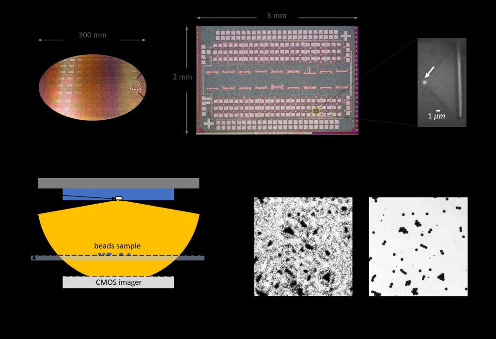
Unlike conventional computational reconstruction methods requiring training data, this neural network does away with the need for training by incorporating a physics model into the algorithm. Alongside holographic image reconstruction, the neural network also enables blind source spectrum recovery from a single diffracted intensity pattern. This represents a significant departure from all previous supervised learning techniques. The researchers envision that the potent combination of CMOS micro-LEDs and the neural network could be beneficial in other computational imaging applications. For instance, they could be used in a compact microscope for live-cell tracking or spectroscopic imaging of biological tissues such as living plants.
“Our breakthrough represents a proof of concept that could be hugely impactful for numerous applications requiring the use of micro-LEDs,” said Iksung Kang, lead author and Research Assistant at MIT. “For instance, this LED could be combined into an array for higher levels of illumination needed for larger-scale applications. In addition, due to the low cost and scalability of microelectronics CMOS processes, this can be done without increasing the system’s complexity, cost, or form factor. This enables us to convert, with relative ease, a mobile phone camera into a holographic microscope of this type. Furthermore, control electronics and even the imager could be integrated into the same chip by exploiting the available electronics in the process, thus creating an ‘all-in-one’ micro-LED that could be transformative for the field.”
“On top of its immense potential in lens-less holography, our new LED has a wide range of other possible applications,” added Rajeev Ram, Principal Investigator at SMART CAMP and DiSTAP, Professor of Electrical Engineering at MIT. “Because its wavelength is within the minimum absorption window of biological tissues, together with its high intensity and nanoscale emission area, our LED could be ideal for bio-imaging and bio-sensing applications, including near-field microscopy and implantable CMOS devices.”
Related Links:
SMART


