Ultracompact Microscope Enables High-Performance Imaging for Biomedical Diagnosis
Posted on 01 Aug 2022
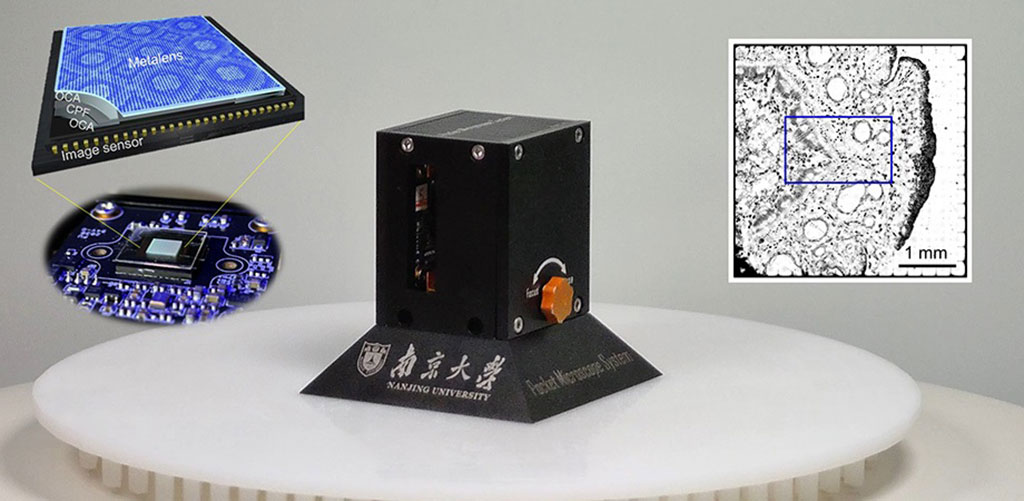
Metalens technology opens a new way to achieve ultracompact and lightweight optical imaging systems. A metalens is a kind of metasurface composed of subwavelength units with powerful capability for manipulating light. An innovative polarization multiplexed metalens array (based on silicon nanoposts) was proposed to realize a compact and wide-field microscope that breaks conventional field-of-view (FOV) constraints, but the imaging quality is relatively poor due to its low efficiency with background noise, and the overall FOV is still smaller than that of traditional microscope with the same resolution. Significantly improved imaging quality is now possible with higher-resolution imaging, thanks to researchers who developed a polarizer-embedded metalens imaging device (PMID).
The PMID developed by researchers from Nanjing University (Jiangsu, China) is implemented based on a silicon nitride metasurface mounted on a CMOS image sensor with a fixed circular-polarization filter inserted between the two. It eliminates background noises, and even enables zoom-in imaging. The new system is based on a special co-and-cross-multiplexed metalens array and embedded polarizer. By integrating them to a chip-scale CMOS sensor, the researchers successfully developed a high-quality wide FOV and large depth-of-field (DOF) microscopy technique.

Significantly high performances are achieved, with a 4×4-mm2 FOV, a 1.74-μm resolution (limited by the CMOS pixel size), and a ~200-μm DOF (450-510-nm wavelength range). This FOV is around 5 to 7 times that of a traditional microscope with the same resolution. The team demonstrated the outstanding microscopy performance by imaging a large number of bio-specimens. This chip-scale microscope promises to revolutionize traditional optical devices, presenting a new horizon of ultracompact imaging devices powered by metatechnology.
“To the best of our knowledge, this is the first time a metalens imager has accessed a larger FOV than a traditional microscope with similar imaging quality,” said Tao Li, senior author and principal investigator at Nanjing University’s National Laboratory of Solid-State Microstructures. “By sweeping the illumination wavelength, the device is able to achieve large depth-of-field imaging simultaneously, thanks to the large dispersive nature of the metalens. This chip-scale PMID enables the implementation of miniaturized portable microscope system, with a thousand-fold reduction in volume and weight compared to a traditional microscope.”
Related Links:
Nanjing University


.jpg)


